

Imagine a chip so dense it packs nearly 100 billion transistors onto a surface smaller than your fingernail — and does it while sipping dramatically less power. That is exactly what IBM claims to have achieved with its newly unveiled sub-1 nanometer chip technology, a research breakthrough that could reshape how AI data centers consume energy and compute power.
What IBM actually announced — and why the number matters
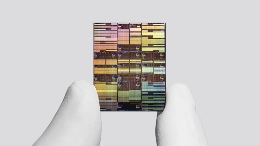
On June 25, 2026, IBM Research revealed what it calls the world’s first sub-1 nanometer chip technology, operating at the 0.7nm node — also referred to as the 7 angstrom node. For context, the “nanometer” in chip manufacturing refers to the size of individual transistors on a chip. Smaller transistors mean more can fit on the same die, enabling faster processing and lower power consumption. IBM’s previous generation was at 2nm. This new node represents a reduction of more than 60% in transistor size.
Why this leap matters for AI data centers
The breakthrough is not aimed at your smartphone or laptop — at least not yet. IBM explicitly targets AI data centers, where the energy demands of training and running large language models have become a growing concern. According to IBM, the new chip architecture can deliver up to 50% more compute performance or up to 70% greater energy efficiency compared to its 2nm chips. For data center operators, that could mean either doubling AI workload capacity within the same power budget, or cutting electricity costs by more than two-thirds for the same workload.
The transistor density revolution — 100 billion on a fingernail
The most striking number in IBM’s announcement is transistor density. The new architecture packs nearly 100 billion transistors onto a chip the size of a human fingernail. That is roughly double the density of IBM’s 2nm node. To put it in perspective: a typical high-end consumer processor today has around 10–20 billion transistors. IBM’s new design crams five to ten times that number into the same physical footprint. This density is achieved through a “revolutionary transistor architecture,” according to IBM’s official statement, though the company has not yet disclosed full technical details of the design.
What Jay Gambetta said — the human voice behind the breakthrough
“It’s not just an incremental step, it’s a meaningful leap forward,” said Jay Gambetta, director of IBM Research and IBM Fellow, in an advance media briefing. He described the technology as “pointing to a future where computing becomes significantly more powerful without a corresponding increase in energy.” Gambetta’s framing is deliberate: the chip industry has long faced the challenge of “dark silicon” — where not all transistors can be powered simultaneously due to thermal and energy constraints. IBM’s claim of simultaneous performance and efficiency gains suggests they have found a way around this fundamental limitation, at least at the research level.
Research stage vs commercial reality — what remains unclear
IBM has been clear that this is a research-stage breakthrough. The company has not announced a timeline for mass production, nor has it named a manufacturing partner. Historically, IBM has licensed its chip technologies to partners like Samsung and GlobalFoundries for commercial production. The 2nm node IBM announced in 2021, for example, took several years to reach prototype stage and has not yet appeared in consumer devices at scale. The same caution applies here: a 0.7nm research chip is a proof of concept, not a product you can buy.
Confirmed facts vs what remains unclear
Confirmed: IBM has fabricated a working test chip at the 0.7nm node. The chip achieves the claimed transistor density and performance/efficiency projections in lab conditions. The announcement was made on June 25, 2026, from IBM’s Yorktown Heights facility.
Unclear: The exact transistor architecture (whether it uses nanosheet, gate-all-around, or something newer). The yield rate — how many chips on a wafer are functional. The timeline for commercial production. The cost per chip. Whether the 70% efficiency gain applies to all workloads or specific AI tasks. IBM has not disclosed these details.
IBM’s moat — why this company can make such a claim
IBM Research has been a pioneer in semiconductor innovation for decades. It invented the first DRAM chip, the first RISC architecture, and the first 7nm test chip in 2015. The company holds thousands of semiconductor patents and has a track record of turning research breakthroughs into licensed technologies. Its moat lies not in manufacturing scale — it sold its chip fabrication plants to GlobalFoundries in 2014 — but in intellectual property and research capability. IBM’s chip designs are used by partners who manufacture at scale. This announcement reinforces IBM’s position as a research leader even as it no longer competes in mass chip production.
Risks and balanced view — the challenges ahead
The semiconductor industry is littered with research breakthroughs that never made it to commercial production. At the 0.7nm scale, quantum tunneling effects become severe — electrons can “leak” across transistor barriers, causing heat and power loss. Manufacturing such tiny features requires extreme ultraviolet (EUV) lithography at wavelengths and precision levels that may not yet be commercially viable. IBM’s 2nm node, announced in 2021, has yet to appear in any major consumer product. Critics may also point out that IBM’s claims are based on internal projections, not independent third-party verification. The company has not published a peer-reviewed paper or disclosed benchmark results.
The broader semiconductor trend — racing below 1nm
IBM is not alone in chasing sub-1nm chips. TSMC has announced plans for 1.4nm (14 angstrom) production by 2028. Intel has outlined a roadmap to 1.4nm by 2027. Samsung is working on 1.4nm as well. IBM’s 0.7nm claim, if validated, would put it ahead of these timelines — but only at the research stage. The broader trend is clear: the industry is pushing toward atomic-scale transistors, where the width of a single silicon atom (about 0.2nm) becomes the ultimate physical limit. IBM’s announcement suggests that limit has not yet been reached.
What this means for AI, energy, and the environment
If IBM’s technology reaches commercial production, the implications for AI are significant. Today, training a single large language model can consume as much electricity as a small town. Data centers already account for roughly 1–2% of global electricity demand, and that share is growing. A chip that delivers 70% better energy efficiency could meaningfully reduce the carbon footprint of AI. For cloud providers like AWS, Google Cloud, and Microsoft Azure — all of whom are IBM partners in various capacities — this could translate into lower operating costs and the ability to offer more compute without expanding data center footprints.
What readers should watch for next
For investors and tech enthusiasts, the key milestones to track are: (1) IBM publishing technical details or a research paper, (2) IBM announcing a manufacturing partner for the 0.7nm node, (3) third-party benchmarks validating the performance and efficiency claims, and (4) any timeline for prototype chips. For students and professionals in semiconductor engineering, this announcement signals that nanosheet or gate-all-around transistor architectures are likely the path forward below 1nm. For the general public, the most immediate impact will be invisible — better AI services running on more efficient hardware, likely years from now.
Future outlook — what could happen next
IBM will likely publish a technical paper detailing the transistor architecture within the next 6–12 months. A manufacturing partnership announcement could follow in 2027, with prototype chips appearing in 2028–2029. Commercial deployment in AI data centers is unlikely before 2030. However, if IBM’s claims hold up under scrutiny, this could accelerate the entire industry’s roadmap below 1nm, forcing competitors like TSMC and Intel to adjust their timelines. The biggest risk is that the technology proves too difficult or expensive to manufacture at scale — a fate that has befallen many promising chip innovations before.
Our Take
IBM’s sub-1nm announcement is genuinely impressive as a research achievement. Packing 100 billion transistors onto a fingernail-sized chip while simultaneously improving performance and efficiency is the kind of breakthrough that semiconductor engineers dream about. But the gap between a lab demonstration and a commercially viable product is vast, and IBM’s track record with the 2nm node — announced in 2021, still not in mass production — should temper expectations. The real significance of this announcement may be less about IBM’s immediate commercial prospects and more about proving that the laws of physics have not yet closed the door on further miniaturization. For an industry that has been warned for two decades that Moore’s Law is dying, IBM just showed it still has a pulse.
Frequently Asked Questions
What is IBM’s sub-1 nanometer chip technology?
It is a research-stage semiconductor breakthrough announced on June 25, 2026, operating at the 0.7nm (7 angstrom) node. The chip packs nearly 100 billion transistors onto a die the size of a human fingernail, offering up to 50% more performance or 70% better energy efficiency than IBM’s previous 2nm chips.
When will IBM’s 0.7nm chip be available for purchase?
IBM has not announced a timeline for commercial production. This is a research-stage breakthrough. Historically, IBM’s chip technologies take several years to reach prototype stage and are typically manufactured by partners. Commercial availability is unlikely before 2030.
How does this compare to TSMC and Intel’s chip roadmaps?
TSMC plans 1.4nm production by 2028, Intel targets 1.4nm by 2027, and Samsung is working on 1.4nm. IBM’s 0.7nm claim is ahead of these timelines but only at the research stage. IBM does not manufacture chips at scale, so its technology would need to be licensed to a foundry partner for production.
Will this chip make my smartphone or laptop faster?
Not directly. IBM is targeting AI data centers with this technology. Consumer devices would benefit only indirectly — through more powerful and energy-efficient cloud AI services. If the technology eventually trickles down to consumer chips, that would be years away.